PCB etching 101
p̞̈͑̚͞c͕͗ͤ̕̕b̬͖̏́͢ ẹ̿͋̒̕t̲̂̓ͩ̑c͕͗ͤ̕̕ḣ̖̻͛̓ỉ͔͖̜͌ṇ̤͛̒̍ĝ̽̓̀͑ 1̨̹̦͍̀0̗̜͕̅̃1̨̹̦͍̀
preparing the image
Preparing an image can be done in software like Fritzing or KiCad. There you will be able to produce the right pin out layout for specific components like arduino and other modules. This allows for the components to be soldered directly onto the board.
1. In Fritzing, open the breadboard tap, drag in the components of your circuit and connect them with wires. this will automatically generate a schematic drawing and PCB layout.
2. Make sure everything is connected properly and then open the PCB tab to arrange the circuit as you please.
3. Export as image (svg/png).
4. Edit your image in an image editor of choice to create a black on white vector image.
lines can be merely decorative or functional, connecting different pin outs.
printing on the copper board
marker method
mimaki flatbed printer
https://static.mywdka.nl/publicationstation/2021/06/25/flatbed-printer-mimaki/
using the uv printer at the interaction station because you can print directly and then etch
! make sure to not print a second protective layer, otherwise you will not be able to clean off the markings after etching !
1. save file as .tiff or .pdf
pen plotter
etching
at the publication station:
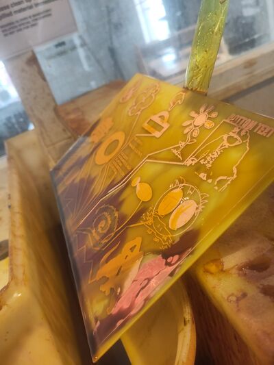
1. Your copper plate with the image will need to be submerged in ferric chloride for around 15 minutes. You need to gently shake it for the copper to corrode.
2. When everything around the drawing is etched off, rinse it with water and then wash it off with soap. The lines covered in marker should now turn copper.
finishing it up
1. clean off the primer with acetone or brush it hard with the green side of a sponge and soap
2. drill pin holes
3. solder components

